Vacuum in the Wake
The “atmospheric” pressure on the near-Earth orbit accommodating satellites is millions of times lower than on the Earth’s surface.
This situation is close to ideal conditions for producing substances which require an extremely clean environment, for instance, semiconductors. Nevertheless, obtaining super pure materials necessary in modern industry requires even higher vacuum. The following solution to this problem exists: to obtain ultrahigh vacuum which is sufficient to speed up the production of mini factory in space to such velocities that substance molecules fail to “catch up” with it
Semiconductors are rather delicate materials: they cardinally change their properties when even a few foreign atoms are added to their structure. This situation is particularly hazardous for thin-film nano-scale coatings (with the thickness smaller than 0.1 µm). That is why such materials should be synthesized in an extremely clean environment, i.e., in the medium containing no oxygen, nitrogen, water vapor, or even inert gases. The best option is high vacuum, because the material purity is directly proportional to the degree of atmospheric rarefaction.
The entire history of vacuum engineering and related technologies presents a permanent and vigorous struggle for super high and pure space vacuum within the tight and rigid framework of on-ground conditions. Each new success in this field has been achieved by mankind against the Earth’s nature, which “is afraid” of emptiness. The cost of modern cryogenic facilities generating superhigh vacuum (residual pressure of the order of 10–12 atm) reaches millions of dollars, and the total cost of development of new facilities can hardly be estimated at all.
The stronger the required rarefaction, the more energy is consumed and the greater amounts of liquid nitrogen and helium are necessary for vacuum equipment operation. In other words, high-vacuum technology is so expensive that deliverying equipment for synthesizing semiconductor nanostructures to space, which is the “storage” of natural vacuum, can turn out to be less expensive in many cases.
More than two thousand years ago, the famous Greek philosopher Aristotel gave an absolutely correct definition of physical vacuum: “Emptiness (vacuum) is the space formed in the wake of a stone thrown by a sling; actually, it disappears instantaneously because particles from the ambient space rush there...” (Terent’ev, 1999). If Aristotel had finished his idea with the statement “…when we accelerate the stone to a velocity commensurable with the velocity of all particles of the ambient medium, there is always an absolutely empty space behind it,” he would have become the inventor of the most advanced method of obtaining super-high vacuumNevertheless, the rarefied gas pressure on the near-Earth orbit, even at the altitude of 1000 km, is at least 10–7 atm, which is insufficient for producing semiconductor nanoelements of required quality. The following solution to this problem exists: superhigh vacuum can be obtained in the wake of an object flying at a high velocity.
Under molecular shield
The idea of obtaining superhigh vacuum was first put forward by the American physicist R. N. Kostoff in 1970. It was only six years later that a team of American researchers headed by L. Melfi performed and published (without citing Kostoff) a theoretical analysis of the state of the gas medium around an object flying in the “airless” space (vacuum) and formulated a concept of an orbital laboratory with a super-rarefied medium inside. These activities were supported by the National Aeronautics and Space Administration of the USA.
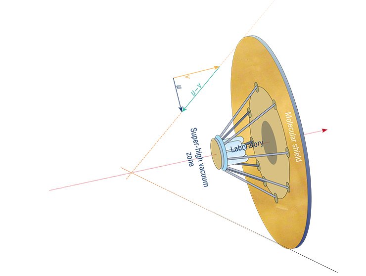
Melfi demonstrated the following: if a protective shield (in the form of a disk or hemisphere aligned transversely to the motion direction) flies in space at a velocity of several kilometers per second, then a conical “wake” practically devoid of matter is formed behind this object. At low orbits, this experiment does not even require large amounts of energy because the usual (orbital) velocity needed for free rotation of the satellite around the Earth has to be reached.
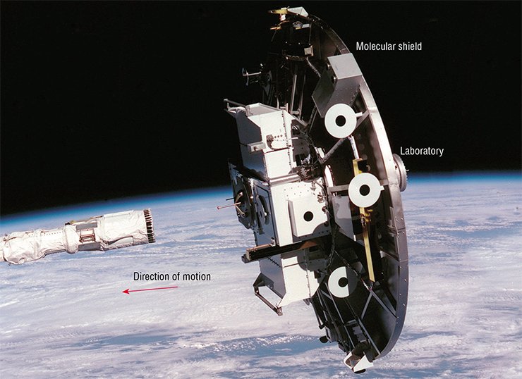
Theoretically, it will take thousands of years for one oxygen molecule (basic species of the gas medium at altitudes of 200—400 km) to appear within 1 m2 area on the back side of such a shield. The total pressure of the medium behind the shield is determined only by scarce molecules of helium and hydrogen (the Sun being the source of these gases) and molecules of substances evaporating from the surface of the shield itself.
In 1989, the Space Vacuum Epitaxy Center (University of Houston) initiated experimental investigations into the possibility of obtaining superhigh vacuum under conditions of open space, aimed at producing semiconductor thin-film multilayered structures. A team supervised by professor A. Ignat’ev constructed a “molecular shield,” which was a steel shield shaped as a disk with laboratory equipment located behind it.
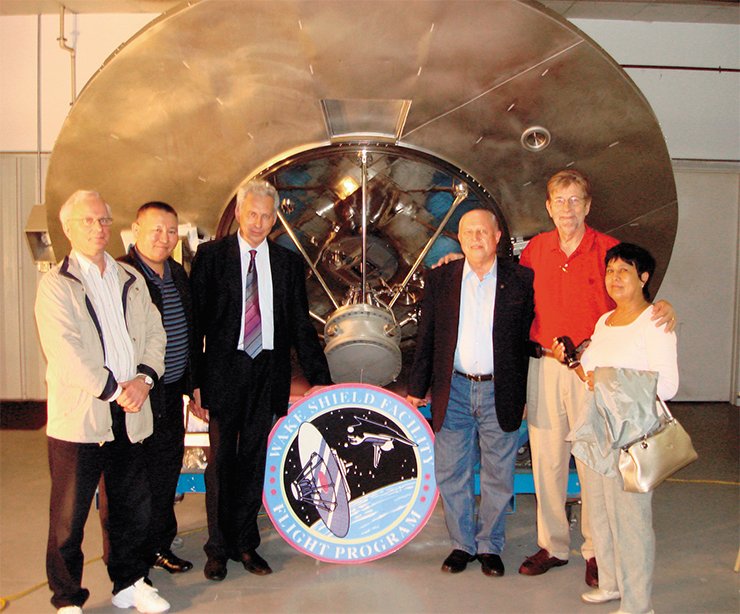
This method is used for producing unique nanostructures, which can be used as the elements of nanoelectronics and nanophotonics in the future, including ultrahigh-frequency transistors, high-sensitivity photodetectors in a wide range of wavelengths, and high-efficiency lasers up to those emitting individual photons
Already the first space experiments provided vacuum with a pressure lower than the ambient pressure by two orders of magnitude. Expensive cryogenic equipment was not required because all species of the gas medium, including inert gases, were rapidly evacuated in a natural way from the working zone of the laboratory under space conditions. Heating of the shield by the Sun assisted in removing pollutants from the shield surface, and cooling in the Earth’s shadow ensured minimization of inherent gas released from the shield material; therefore, superlow pressure was stable during the synthesis of semiconductor films.
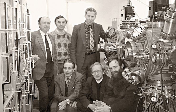
Three series of full-scale experiments performed in 1994—1996 provided a large amount of important scientific and engineering information on the possibility of obtaining unique semiconductor materials in the open space, where principal constraints of ground-based vacuum technological processes are eliminated. After the tragic accident with the Columbia shuttle crew in 2003, however, American experiments were suspended.
Russians do not fall behind
Research activities aimed at using space vacuum for growing semiconductor thin-film multilayered systems and nanostructure have been performed not only in the USA. One of the leaders in the field of super-high vacuum technology and equipment in our country is the Rzhanov Institute of Semiconductor Physics (ISP) of the Siberian Branch of the Russian Academy of Sciences (SB RAS) in Novosibirsk. Its research activities include industry-oriented production of multilayered thin-film semiconductor materials, in particular, by the molecular-beam epitaxy method.
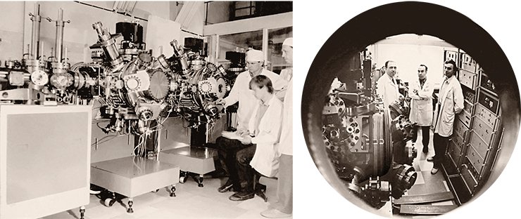
The Ekran (shield) project proposed by the institute for growing thin-film compositions on the Russian orbital system Mir was first considered at a meeting of the Department of Space Material Science of the Council on Space of the Russian Academy of Sciences in 1995 and was approved by experts. Soon the first simulator of space vacuum was designed and fabricated in Novosibirsk on the request of the International Scientific and Technical Center of Payloads of Space-Based Facilities (Mytishchi) and Rocket Space Corporation Energia (Korolev). Within the framework of the Epitaksiya (Epitaxy) program of the Department of Basic Space Research RAS and the contract on very important activities for governmental purposes, ISP SB RAS developed and tested process equipment for growing semiconductor films under open space conditions.
As for the shield providing superhigh vacuum, its creation was a result of successful cooperation between institutes, departments, and even states. Thus, the Khristianovich Institute of Theoretical and Applied Mechanics SB RAS (Novosibirsk) performed gas-dynamic calculations of various shield shapes. Specialists from the International Scientific and Technical Center of Payloads of Space-Based Facilities and the Rocket Space Corporation Energia performed experimental and theoretical investigations into the state of the gas medium around space objects on which the shield was to be mounted. They also developed a unique structure of the shield and the measurement equipment. The pilot sample was fabricated at the Paton Electric Welding Institute (Kiev, Ukraine). Creation of energy supply systems and onboard means of automation and telemetry was the responsibility of the Department of System Engineering (ISP SB RAS), for the on-ground version and the Elektron (Electron) company (Krasnoyarsk) for the space version.

In contrast to the American flat shield, our shield looked as a laced “umbrella.” A multilayered foil with a special coating preventing surface evaporation was pulled on the spokes of this umbrella. The first tests of the structural elements of the molecular shield were successfully performed on the Mir orbital station in 1998: the shield material survived in the open space even when the Earth passed through the Leonidas meteor shower.
Yet, further plans of scientists were never realized: on 21 March, 2001, the Mir orbital station was sunk in the Pacific Ocean. Subsequently, financing of space projects was terminated.
Nevertheless, this is not the end of the story. In 2004, the Memorandum on Cooperation in the field of space material science was signed between the University of Houston and ISP SB RAS. The Ekran project became international. In two years, the Kazakh Institute of Physics and Technology (Almaty) joined the team. ISP SB RAS revived activities aimed at developing new scientific equipment for experiments on epitaxy, now under conditions of the Russian segment of the International Space Station (ISS).
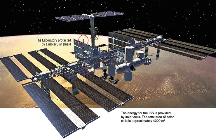
In 2006—2009, within the framework of activities on the project at the Pilot Plant SB RAS and pilot production of ISP SB RAS, with participation of the Technological Design Institute of Scientific Instrument Engineering SB RAS, two sets of on-ground super-high vacuum equipment for growing semiconductor nanostructures were fabricated. These facilities were installed at the Novosibirsk State Technical University and Tomsk State University.
The forthcoming stage of joint activities includes on-ground experiments on testing the technology of synthesizing various semiconductor nanoelements for electronic instruments and photosensitive equipment. For this purpose, ISP SB RAS has developed a simulator of space vacuum called Epitsentr (Epicenter), which is now undergoing laboratory tests. A copy of this equipment is planned to be installed at the Chair of Engineering Physics of the Siberian Aerospace University (Krasnoyarsk), where specialists in new space technology will be trained. Further fabrication of similar equipment for the American and Kazakh parties is planned.
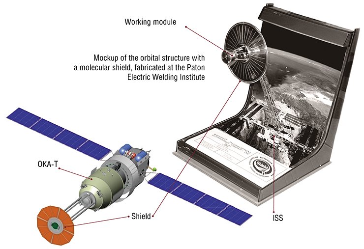
Vacuum is needed not only for production of semiconductors. There are certain chemical and biochemical processes which are extremely sensitive to minor amounts of admixtures in the medium. In the future, space vacuum technologies can also be used in versatile (sometimes, unexpected) fields.
In the short-term prospects, however, the main commercial benefits of this technology are related to high-efficiency solar cells production. The demand for such cells is extremely high in space environment, which has no other sources of energy. Owing to such facilities as the molecular shield, it will be possible to fabricate these solar cells directly on the orbit and use them there as well.
References
Berzhatyj V. I. i dr. Perspektivy realizacii vakuum¬nyh tehnologij v uslovijah orbital’nogo poleta // Avtomaticheskaja svarka, 1999. № 10. S. 108—116 //Poverhnost’, 2001. № 9. s. 63—72.
Pcheljakov O. P. i dr. Poluprovodnikovye vakuumnye tehno¬logii v kosmicheskom prostranstve: istorija, sostojanie, perspektivy // Poverhnost’, 2004. № 6. s. 69—76.
Terent’ev M. V. Ob istorii i razvitii ponjatija fizicheskogo vakuuma. M.: Fazis, 1999.
Pchelyakov O. P. et al. Epitaxy of compound semiconductor from molecular beams in space vacuum behind molecular shield. Proc. of Joint X Europ. and VI Russian symp. on Phys. Sci. in Microgravity. On physical sciences in microgravity, 1997. V. II. P. 144—149.
Strozier J. A. et al. Wake vacuum measurement and analysis for the wake shield facility free flying platform // Vacuum. 2002 V. 64. P. 119—144.
The paper includes photographs from the archives of the author and V. Novikov


