Siberian Nanoforum
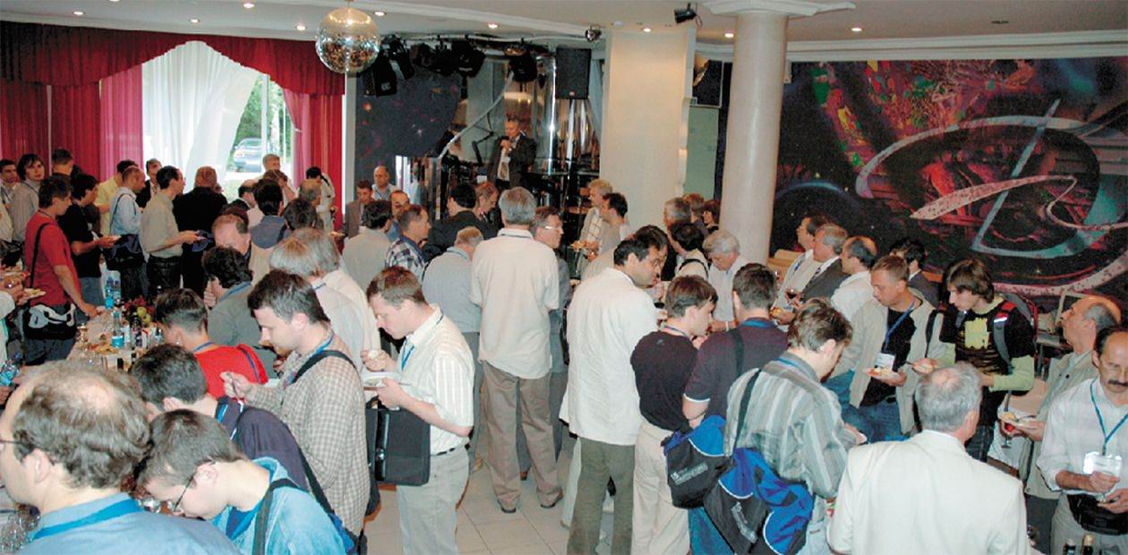
The annual International Symposium on nanostructures, scheduled to coincide with celebrations of the 50th anniversary of the Siberian Branch of the Russian Academy of Sciences, was held in the Novosibirsk Academgorodok on June 25—29, 2007
Development of modern semiconductor nanotechnologies in Russia depends on intense interaction of scientists in this country and their cooperation with foreign colleagues. The first International symposium on semiconductor nanostructures was organized in 1993 by academician Zh. I. Alferof, Nobel prize winner, on the basis of the Ioffe Physicotechnical Institute in St. Petersburg. Since that time, at the end of June every year, specialists of the leading institutes of central Russia, Siberia, and the Far East working in this field have been coming together to discuss the modern trends in nanotechnologies and nanophysics, to share the latest scientific news, and to learn the experience of colleagues from the leading scientific schools of Europe, USA, and Japan.
This year it was decided to hold the symposium in Novosibirsk, at the Institute of Semiconductor Physics of the Siberian Branch of the Russian Academy of Sciences. The Director of the institute, Academician A. L. Aseev, believes that this decision allowed all participants to get acquainted with the leading institute of Siberia in the field of semiconductor nanotechnologies as well as with the beauty of Siberia. More than 200 scientists from all over the world took part in the symposium, and it was encouraging to see many young scientists.
The main topic of the forum was the new achievements in physics of nanostructures, nanotechnologies, and prospects of practical applications of these achievements.
“Whiskered” fireflies
It is impossible to tell about the details of all scientific directions discussed in the presentations of symposium participants. Let us mention those which attracted the most attention. The conference was opened by an interesting presentation of Prof. Chang-Hasnain from the University of California (Berkley). He spoke about the manufacturing of laser diodes on the basis of light-emitting nanowires from gallium arsenide (GaAs) and indium phosphide (InP) grown on a silicon substrate (Si). As was noted by the speaker, the growth of nanowires is initiated by spraying, in vacuum, a small amount of gold (Au) which forms liquid nanodrops of Au-Si of the eutectic as the temperature is increased to 450 °С, so that the growth of “whiskers” (nanowires) occurs under the eutectic droplets upward from the substrate. By varying the ratio of the flows of the original components, one can change not only the droplet diameter, but also (which is most surprising) the droplet shape: from cylindrical to conical.
Each nanowire is a light-emitting element. Yet, as the wire diameters are very small (tens of nanometers), their electron-optical properties become dependent on the size and shape by virtue of quantum restrictions. This is manifested in a significant “blue” shift of the luminescence band, which means a change in the wavelength of the emitted light toward shorter wavelengths.
The possibilities of the technology developed are so wide that it is possible to create singular quantum dots from another material, e. g., InAs, inside InP nanowires; these quantum dots not only possess a narrow emission width of 1 meV (millielectronvolts), but also are responsible for luminescence of structures at room temperature. This opens the way for practical applications of such nanowires as light-emitting elements.
Memorial rings
T. Mano, a Japanese scientist, told about a new method of “droplet eptaxy,” a method of creating nanometer-sized ring structures, one of the versions of the idea of self-formation, which has been used for production of quantum dots for more than 15 years. The essence of this idea implies that the growth of a film of one semiconductor material on a “foreign” substrate made of another material may be unstable, and the growing film, beginning from a certain thickness, is split into tiny islands. These are the quantum dots (QDs). In practice, such dots are expected to be used as the working elements of semiconductor lasers, flash memory, and even elementary “bricks” of a quantum computer.
The method proposed can also be used for creating another class of nanoobjects (quantum rings), which are also very interesting. This implies the growth of a gallium arsenide film, where fluxes of gallium atoms and arsenic molecules are directed onto the growing surface under conditions of superhigh vacuum. The essence of the method is as follows: at a certain time, the flux of arsenic is interrupted, and the excess gallium on the surface gathers into droplets approximately 50 nm in size. Then arsenic is supplied again, while the flux of gallium is interrupted. The incoming atoms of arsenic “run” over the surface, find gallium droplets, and react with the latter. As a result, a “rim” of gallium arsenide, i. e., a quantum ring is formed around each droplet.
By varying the growth conditions, one can also obtain double quantum rings, where an additional outer ring is formed owing to atomic gallium and arsenic fluxes directed toward each other. These quantum rings, being placed into a magnetic field, can demonstrate effects of interference of electron waves. Note that similar quantum rings (made, actually, by different technology) are also studied at our institute. In particular, we developed a ring quantum interferometer of a record-beating small size.
Electron billiards in a microwave oven
A French scientist, S. Sassine (Grenoble), who was awarded as the best young speaker, told about experiments with the so-called electron billiards affected by a microwave field. This billiards is arranged as follows: antidots are etched in a semiconductor structure with two-dimensional electron gas. These antidots are fragments in the form of semicircles arranged into a regular grid. As a result, electrons can “run” between these semicircles, being specularly reflected from the latter.
It turns out that, if such a structure is subjected to microwave radiation, a d. c. current flows in the direction where the semicircles are “looking.” The authors themselves call this phenomenon the “ratchet effect,” meaning that the main thing here is the violation of symmetry. Like the ratchet-wheel in the clockwork, which can rotate in one direction only, the electrons in the examined system can move only in a certain direction with different types of reflection from the flat and rounded sides of the antidot. In this case, microwave radiation serves to “swing” the electrons, the effect being dependent on wave polarization. In the author’s opinion, such a device can be used as a polarization detector.
It should be noted that this research direction (studying electron billiards with antidot grids) appeared and is developing thanks to the works of scientists from the Novosibirsk Institute of Semiconductor Physics (ISP). Thus, the talk given by A. G. Pogosov, an ISP research worker, was devoted to the mysterious behavior of billiards resistance in a magnetic field. This experimental work has yet to be theoretically justified.
Terahertz surfing
Of great interest for symposium participants was the presentation of the young ISP researcher E. V. Naumova, who spoke about using microhelices to control polarization of terahertz waves (a terahertz is equal to 1 012 hertz’s, which corresponds to a wavelength of about 100 microns). This was a joint project of two teams: the Institute of Semiconductor Physics, where a method of extremely precise and controlled creation of three-dimensional micro- and nano-objects was invented and is widely developed, and the Institute of Nuclear Physics, which possesses a unique source of terahertz radiation: a laser on free electrons.
The essence of the experiment was transmission of radiation with a frequency of several terahertz through small gilded helices (several tens of microns) aligned evenly on a semiconductor substrate. The measured parameter was polarization, i. e., the direction of the electric field of the transmitted wave. What is it needed for? The point is that the terahertz range, which lies in the scale of electromagnetic waves between the microwave radio waves and infrared light, has not been adequately studied. For light waves, for instance, there is a method of controlled rotation of the polarization plane with the help of liquid crystals: this is the principle of operation of LCD monitors. Nothing like that was proposed for terahertz waves. It was in this direction that the ISP scientists made their first step:” they demonstrated that a layer of microhelices can rotate the polarization plane of terahertz waves, which results in changing the direction of the electric field.
The idea is obvious: it has been known for a long time that light changes its polarization when passing through a medium containing helically swirled molecules, for instance, through a solution of sugar. For the terahertz range, however, helical molecules cannot be used: they are too small. Therefore, hand-made helices prepared under rigid “technological norms” are needed: deviations of the helix size and diameter should be rather small.
Here one cannot avoid the technology developed at ISP, in the laboratory headed by V. Ya. Prinz*. The general idea of this technology is as follows: a two-layer film is prepared, with internal elastic stresses which make this film bend. While the film attached to the substrate is not yet bent, the required “patches” are “cut out” from this film; for instance, to obtain helices, one has to cut out rectangles at an angle to crystallographic axes. Then the film is liberated by means of etching and coils into a required structure.
That was how nanoelements needed for the experiment were obtained. The researchers are further planning to create an unusual substance, a multilayer (bulk) metamaterial with a negative refractive index of terahertz radiation, moreover, a metamaterial capable of dynamic “switching” for superfast control of polarization, amplitude, and direction of wave propagation.
The future of “quantum dots”
Prof. D. Bimberg (Berlin), who opened the final plenary session of the conference, gave a brilliant presentation of the results of research performed within the framework of wide-scale cooperation of German and Russian scientists. The speaker discussed the prospects of using semiconductor nanostructures (quantum dots) for creating superfast memory chips and reliable systems for protection of computer systems.
Such devices are intended to operate at room temperature, which is a complicated problem because quantum effects forming the basis of nanoelectronics decay with increasing temperature. The main requirements imposed on such devices are the possibility of storing charge carriers (information) for a long time (years), a very small (about 1 ns) time of recording, and the possibility of multiple (about 1 015) cycles of recording and erasing information.
All these requirements will be probably satisfied by quantum dots made of semiconductor materials of the third and fifth groups (arsenides of indium, gallium, etc.), but not the usual ones.
Normally, QDs are obtained by the known Stranski-Krastanov mechanism, where a strongly stressed continuous film transforms to a system of pyramidal islands. In our case, however, these are extremely thin islands of a foreign material obtained by sub-monolayer deposition of the substance, which are multiply inserted into the layers of the basic material. By varying the composition of sub-monolayer quantum dots and the material surrounding them, one can expect the time of information storage to increase to several years, which is fairly optimistic in terms of the prospects of semiconductor nanoelectronics.
Even more astonishing perspectives are associated with the use of individual QDs as single-photon emitters in quantum cryptography, comparatively recent research activities which allow of application of the effects of quantum physics to create secret channels of data transfer with reliable protection from interception, for the fundamental feature of quantum systems is that it is impossible to detect their state precisely.
A. V. Nenashev, candidate of physics and mathematics,
D. V. Shcheglov, candidate of physics and mathematics,
L. I. Fedina, candidate of physics and mathematics
The authors and Editorial Board of the journal would like to thank A. V. Latyshev, doctor of physics and mathematics, for his help in preparation of the article.
*See: SCIENCE First Hand, 2007, № 2 (14)


