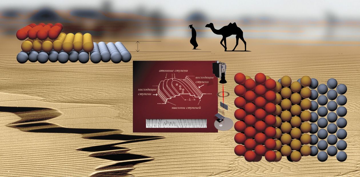
Up and Down Atomic Steps
or how to pass from surface science to nanoscale measurements
For us any view of a material object starts from its surface, which is, in fact, the boundary separating the object from the environment. For any technology it is essential to study surface properties and find a way to control them. The possibility of observing directly the dynamic behavior of object surfaces at the nanoscale has appeared owing to the combination of reflection electron microscopy and ultra-high vacuum techniques
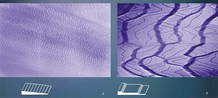
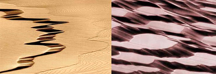 This is not the surface of Mars. This is the view of a clean surface of crystalline silicon after heating the crystal with the direct electric current to 1300°С. The image was produced in a reflection electron microscope (REM) at 30,000 magnification
A strange, fantastic relief with a countless number of dunes that have abruptly ending edges… This is not the surface of Mars or another extraterrestrial object. Scientifically speaking, this is a reflection electron microscope (REM) image (30,000 magnification) of the atomically clean surface of a single crystal silicon (Si) slab after the prolonged application of the electric current heating the crystal to 1300°С. We will return to the reasons for the appearance of such an unusual relief later, and for now let us literally stay on the surface.
There is no need to mention the fact that surface properties are of great importance; it is the surface that defines the start and end of any object or technology. When researchers learned how to change the electronic properties of the near-surface regions of silicon crystals by doping and covering them with silicon oxide and metal and, as a result, to produce transistors, they triggered the development of silicon microelectronics. Already then the characteristics of the produced devices were largely determined by the properties of the surface itself and of the interface, including the presence of impurities.
Today, based on the current technologies using the prefix nano-, new instruments are made; they operate at a depth of several tens of atomic layers, in fact, on the surface. These technologies impose more rigid requirements on the quality of the surface and on the control of atomic processes occurring on it. Therefore, it is impossible to do without profound knowledge about the atomic motion on the crystal surface and about the interaction of atoms with atomic steps, which are the main structural element of the crystal surface. However, in order to study these processes, an appropriate method that will enable the visualization of the surface structure is required. One of these structure sensitive methods is REM.
Silicon “stairs”
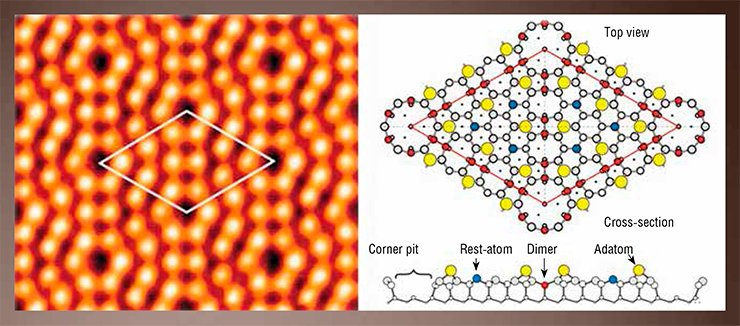
The REM images of atomic steps on the real silicon surface as well as the computer simulated structural model reveal that the steps are caused by the protrusion of crystallographic planes with increased atomic density on the surface.
How does it happen? Just imagine that you cut a crystal in which, as you know, all atoms are strictly ordered in the form of a three-dimensional lattice in accordance with the type of chemical bond. In the simplest case, such a lattice consists of elementary cubes whose corners and faces contain atoms. This cube is called a unit cell; its translation over three spatial coordinates reproduces the positions of all atoms in the crystal lattice.
Atoms in the silicon lattice are covalently bonded, which results in a diamond-like structure characteristic of all Group 4 elements of the Mendeleev Table. In terms of unit cells, the diamond structure consists of two cubes inserted into each other along the cube diagonal, to one-fourth of its length.
In order to describe diverse crystal lattice sections in which the atomic density considerably varies, Miller indices are used. Without going into detail, let us only say that the Si surface with the (111) indices corresponds to the section of the double cube along one of its diagonals. Theoretically, in the case of such a precise section (parallel to (111) planes) it is possible to produce an ideal atomically smooth surface without any steps.
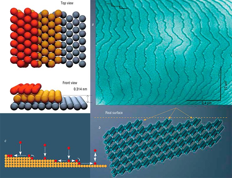 However, in reality it is impossible to cut the Si ingot precisely along the (111) plane because the current cutting accuracy does not exceed 0.5°. This means that the real surface of the cut crystal consists of parts of atomically smooth regions of the (111) surface divided by atomic steps, which is well seen in the computer model. The height of the steps that emerge is strictly equal to the distance between the (111) planes on the surface, i.e., 0.314 nm. In fact, this distance is close to the size of the silicon atom per se (~0.1 nm or 10–10 m); therefore, the steps are called atomic.
Thus, the real atomically clean Si (111) surface reminds a staircase in a house, where the surface of the step on which a foot is placed is an atomically smooth terrace, while its edge is an atomic step proper into which atoms are embedded or out of which they come during crystal growth or during sublimation processes, respectively.
Super vacuum in a “matchbox”
It is very difficult to see atomic steps because of their low height, comparable with atom sizes; therefore, for a long time they were objects of purely theoretical studies. For the first time, the experimental image of an atomic step made by REM under super vacuum conditions was shown by Prof. K. Yagi (Japan) at a Congress on Crystal Growth in Moscow in 1980.
Since that time the REM method has been actively developed at the Institute of Semiconductor Physics, Siberian Branch, Russian Academy of Sciences, Novosibirsk. This was initiated by S. I. Stenin, Head of the Laboratory of Electron Microscopy. Owing to his efforts, at that time the Institute already had the prerequisites for a breakthrough in creating large super vacuum installations that predetermined the rapid development of the molecular beam epitaxial technology, which enabled the growth of perfect single crystal layers of compounds on a substrate. The capabilities of the REM method ideally complied with the problems of this technology because growing epitaxial structures required detailed information about the elementary processes of atom attachment to and detachment from atomic steps, which underlay the epitaxial growth process.
REM is based on conventional transmission electron microscopy; however, the object under study is located here at a small (~5°) angle relative to the electron beam. One of the first scientists who put forward this idea as far back as the 1930s was the German physicist Ernst Ruska. Later he was awarded with the Nobel Prize for theoretical works in electron optics and for creating the first electron microscope. However, at that time the researchers could not fully implement the idea of REM because it was impossible to get a good vacuum in the microscope column. Nonetheless, having turned the thin sample at an angle of 90° relative to the electron beam, which in this case was able to pass through all the thickness of the sample, Ruska managed to design a transmission electron microscope, which is now the main instrument in the materials science.
Silicon is second to oxygen in abundance in the Earth’s crust; however, in nature it mainly occurs in the form of various compounds based on silicon dioxide and also silicates and aluminosilicatesSingle crystal silicon, the basis of microelectronics, is produced artificially in the form of ingots. At present, this is the purest material that has ever been produced by people. However, it is possible to create and observe the atomically clean surface of a silicon sample only after its sublimation in a super-high vacuum
In order to observe atomic steps on the silicon surface by means of REM, especially in situ, it was necessary to create an ultrahigh vacuum (UHV) around the sample. Yet another problem to be solved was cleaning the sample from natural oxide that inevitably appeared on the silicon surface as a result of interaction with atmospheric oxygen. The problem is solved by heating the sample to the sublimation temperature of the material (about 1300 °С), e.g., by passing the electric current.
Thus, to observe atomic steps on the silicon surface, a small UHV-cell with two apertures for the electron beam to come into and out was needed. Inside the UHV-chamber, there had to be a sample which could be heated up to 1300 °С, along with a substance deposition source. In order to create UHV, the walls of the chamber had to be cooled by liquid nitrogen, the opportunity to perform mechanical adjustment of the electron microscope lenses being preserved.
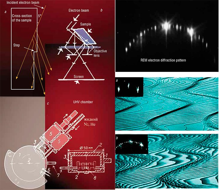 It was an incredible challenge to design a very complicated device of a matchbox size which could be inserted in a small space inside the electron microscope. By joint efforts of gifted scientists and engineers (S. I. Stenin, A. L. Aseev, A. V. Latyshev, A. B. Krasil’nikov, B. Z. Kanter, A. A. Kroshkov, E. A. Baranova, O. A. Yakushenko, N. I. Kozlov, I. N. Sizikov, and V. V. Reshetnikov) the problem was successfully solved. This work still does not have any analogues in the world.
At present, the SB RAS Institute of Semiconductor Physics in Novosibirsk is the only place in the world where the UHV REM method is applied in situ to study the atomic processes on the crystal surface. The method makes it possible to perform successful experiments on investigating the structure and morphology of atomically clean crystal surfaces during sublimation, epitaxy, oxidation, catalytic reactions, and other processes that can be carried out in the UHV REM cell.
 It is worth noting that now interest in the studies in situ is growing worldwide, and the leading manufacturers of electron microscopes are actively developing various embedded cells to examine the processes in working nanoinstruments.
The longer the step bunch, the slower it moves
One of the most outstanding theoretical discoveries made in the 1980s by means of in situ UHV REM was the step bunching effect (Latyshev, Aseev, et al., 1988; Latyshev, Krasil’nikov, et al., 1988; Latyshev et al., 1989; 1991; 1994). This discovery not only anticipated the theory but also proved to be very useful for performing accurate measurements in the nanoscale (1—100 nm).
The fact is that a system of moving atomic steps that are equidistantly located on the clean silicon surface becomes unstable after being heated by the direct current to the sublimation temperatures. Under certain conditions, it rapidly transforms into clusters of steps called bunches, by analogy with a train set of cars. The more atomic steps (cars) cluster in the bunch, the slower it moves.
 Since each atomic step is related to a particular atomic altitude difference on the surface, the bunch height is determined by the number of clustered steps. Consequently, the surface relief changes radically and becomes a well developed, even rough, “Martian” relief. In fact, step bunches are natural nanostructures on the crystal surface whose height is strictly multiple to the height of a separate atomic step. Therefore, as will be shown further, they can be used for making accurate measurements in the nanoscale.
The step bunching effect turned out to be reversible. It depends on both the current value (temperature) and its direction; hence, by changing these parameters it is possible to purposefully alter the step bunch shape (i.e. the distance between the steps) up to their complete destruction and to the reconstruction of the initial step distribution.
The initial stage of clustering the steps that move, at first, at a constant rate can be compared to a traffic jam near traffic lights, which, in our case, switch on when the temperature or current direction is changed. However, the microscopic nature of such jams on the surface still remains unclear. They are assumed to be associated with changes in the processes of atom attachment to and detachment from the steps in the event of current switching, and also in the event of partial ionization of atoms moving on the surface and entrained by the electric field applied to the sample (Latyshev et al., 1996; Latyshev and Aseev, 1998).
Self-organization of the nanorelief
Well after the discovery of the step bunching effect, it became clear that the morphological instability of the surface, i.e., the appearance of the nanorelief, is a general manifestation of the surface self-organization process because it is observed in diverse conditions: during sublimation, epitaxy, crystal growth, and even inside a solid during solid phase crystallization. This implies that the morphological instability appears on the surface and on the interfaces non-randomly, and is caused by a decrease in the energy of the system when certain factors are in action.
In other words, the formation process of natural nano objects on the surface due to its self-organization is as inevitable under certain effects as the origin of a living cell (in essence, a complex bionanostructure) in the course of evolution of our planet. Since the physical properties of objects with sizes ranging from 1 nm to 100 nm are known to differ drastically from their macro analogues, this phenomenon can be used to create quite new devices and instruments based on other physical principles. In this respect, the processes when nanostructures appear due to the natural redistribution and self-organization of atoms are of great practical interest from the standpoint of the development of nanotechnologies by the bottom-up type in the size scale.
The clustering of atomic steps is so intricate that it has not been completely explained so far because the microscopic parameters that describe the atom attachment to and detachment from the steps are hard to determine even by means of in situ REM. Moreover, the theory predicts nonequivalence of the atom attachment to a step from the upper and lower terraces.
Furthermore, theoretically, atoms can freely move along a step without any attachment; in this case, the step is transparent. However, atoms attach immediately to a single jog of the atomic step (a step as well as a line can be straight or can contain atomic jogs). If there is no inflection, i.e., for strictly rectilinear parts of the steps, atom attachment is hindered. All this was shown by another very interesting in situ method: scanning tunneling microscopy (STM), which enables the visualization of the surface atomic structure at temperatures below 600°С.
The general process of atom attachment to a step, which is sufficiently sophisticated, is dramatized by the appearance of the so-called superstructure on atomically smooth terraces (i.e., between the steps) if the temperature is decreased to 830°С. This phenomenon is associated with collective rearrangement of the surface atoms, including the formation of new bonds not characteristic of bulky atoms. Hence, the unit cell size in the surface superstructure increases several times as compared with that observed in the crystal bulk. The formation of a superstructure is a typical example of surface self-organization when its energy decreases because of the minimization of the number of broken atomic bonds.
As a result of all these processes, a very complex structure whose translation period is seven times larger than that of the initial surface appears on the Si (111) surface at a low (< 30 °C) temperature. The formation of the superstructure (7×7) is easy to visualize in the REM image owing to highly blurred shadows appearing near the atomic steps. In the diffraction image made in another mode of electron microscope lenses, there appear small reflections between the main pronounced diffraction reflections, dividing the distance between them into exactly seven intervals.
The application of the in situ REM method, using the step bunching effect, proved to be very informative for studying the atom attachment to a step if there exists a superstructure (Roghilo et al., 2013).
At first, the dense array of steps gives rise to the formation of wide atomically smooth terraces separated by step bunches. The bunch to the right of the atomically smooth terrace consists of ascending steps, while the left bunch consists of descending steps.
The subsequent deposition of silicon atoms results in the nucleation of small two-dimensional islands in the center of smooth terraces, which are visualized as dark dots in the REM image. Near the step bunches, depletion regions of different width are formed, within whose limits islands are not generated. This phenomenon demonstrates the non-equivalence of atom attachment to ascending and descending steps. The fact that the depletion zone is larger near the descending steps indicates the preferential atom attachment to these steps and is consistent with the current theoretical models of epitaxial growth.
Further growth is accompanied by the formation of a pyramidal structure limited by zigzag steps with long rectilinear parts. Visualizing the process of atom attachment to a step at the atomic level by means of the above-mentioned in situ STM, but magnifying it several million times, it is possible to see* that the formation of rectilinear steps is caused by the rapid attachment of atoms to single jogs. However, atom attachment to a rectilinear step turns out to be extremely hindered.
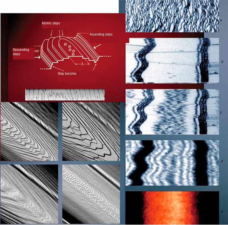 The analysis of the growth process of the pyramidal structure depending on the formation conditions (terrace width, temperature, and deposition rate) made it possible to determine the value of the energy barrier for the atom attachment to a descending step. It also became possible to show that step transparency is a real phenomenon which is due to the fact that atom attachment to rectilinear parts of the steps is limited. This important information must give us insight into the step bunching mechanism, and further application of the in situ REM method will certainly bring many new useful results.
How to measure the nano
Developing nanotechnologies and manufacturing nanoproducts require a reliable standardized method to measure the sizes of the produced structures (including vertical) in the range from 100 nm to the atomic size (0.1 nm). To this end, not only special instruments are necessary, such as an atomic force microscope (AFM), but also gauge samples for adjustment. The current metrological system that uses the meter as the standard of length is of no use for this size scale.
The other linear measures developed so far are based on lithographic methods (the so-called top-down technologies, from macro- to nanosizes by cutting the odds); they have a minimum size of 525 nm, which is too much. Actually, the ideal candidate for elaborating metrological linear measures in the nanoscale is the bunch of steps that appears in the self-organization conditions of the atomically clean surface. Since the bunch height on the Si (111) surface is strictly multiple to the height of a separate atomic step, the bunch height can be determined with high accuracy.
Recently the height of an atomic step on the real Si (111) surface covered with a thin layer of natural oxide was directly measured with atomic resolution in a high-resolution electron microscope to find that it is 0.314 ±0.001 nm, which corresponds to the distance between the Si (111) crystallographic planes (Fedina et al., 2010). X-rays helped to measure this parameter with an even higher accuracy, up to the eighth digit after the dot. Therefore, both the atomic step and the atom itself can be considered as natural constants of linear sizes in the nanoscale.
There is only one problem created by the high density of atomic steps on the surface after the industrial cutting or chipping of the crystal, which does not allow us to use these surfaces for calibrating AFM. Therefore the phenomenon of atomic step bunching is so important: it makes it possible to create surface areas with different densities of atomic steps. By creating wide atomically smooth parts with a single atomic step and an step bunch with a countable number of steps, it is easy to produce a sample for measurements in any height range.
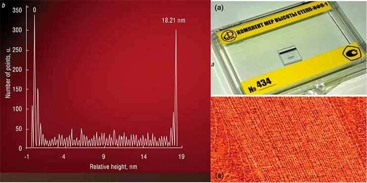 Currently, the in situ REM method demonstrates a direct transition from the study of phenomena that occur on the atomically clean surface of the crystal to practical application of the knowledge obtained. The new knowledge offers opportunities for controlling the processes of growth and for making semiconductor materials that possess the properties required for modern micro- and nanoelectronics.
As for the direct practical application of the results of investigations based on in situ REM, the Institute of Semiconductor Physics (Siberian Branch, Russian Academy of Sciences, Novosibirsk) already has standard samples that enable high-accuracy measurements in the nanoscale with respect to the height of a separate atomic step. After passing the state tests, the set of high-accuracy measures of vertical sizes (STEPP-IFP-1) was included in the State Register of Measuring by Russian Standard order No. 6290 of October 31, 2011.
*See the orginal video at http://www.fz-juelich.de/pgi/pgi-3/EN/UeberUns/Organisation/Gruppe2/STM-Movies/artikel.html
References
Latyshev A. V., Aseev A. L., Krasil’nikov A. B. i dr. // Doklady AN SSSR. 1988. T. 300. № 1. S. 84.
Latyshev A. V., Krasil’nikov A. B., Aseev A. L., Stenin S. I. // Pis’ma v ZhJeTF. 1988. T. 49. № 9. S. 448.,
Latyshev A. V., Aseev A. L. // Uspehi fizicheskih nauk. 1998. T. 168, № 10. S. 1117.
Latyshev A. V., Aseev A. L. Monoatomnye stupeni na poverhnosti kremnija. Izdatel’stvo SO RAN, 2006. 242 s.
Fedina L. I., Sheglov D. V., Kosolobov S. S. et al. //Meas. Sci. Technol. 2010. V. 21. P. 054004.
Rogilo D. I., Fedina L. I., Kosolobov S. S., et al. // Phys. Rev. Lett. 2013. V. 111, P. 036105.
Latyshev A. V., Aseev A. L., Krasilnikov A. B., and Stenin S. I. // Surf. Sci. 1989. V. 213. P. 157.
Latyshev A. V., Krasilnikov A. B., Sokolov L. V., et al. // Surf. Sci. 1991. V. 254. P. 90.
Latyshev A. ., Krasilnikov A. B., Aseev A. L. // Surf. Sci. 1994. V. 311. P. 395.
Latyshev A. V., Minoda H., Tanishiro Y., and Yagi K. // Phys. Rev. Lett. 1996. V. 76. No. 1. P. 94.
The work was supported in part by the Russian Foundation for Basic Research, project No. 14-22-00143.
The authors are grateful to Dr. S. S. Kosolobov, Dr. D. I. Shcheglov, Prof. A. D. Shklyaev, and post-graduate D. I. Roghilo (Institute of Semiconductor Physics, SB RAS, Novosibirsk) for their assistance in preparing the publication.


