Nanotube, Light Up!
The schematic circuit of a traditional electrical lamp includes a radiating element connected by two wires supplying an electrical current. Siberian scientists have created a hybrid nanomaterial based on carbon nanotubes; it requires only one electrical contact for luminescence. The efficiency and economy of the device has only increased
The schematic circuit of a traditional electrical lamp includes a radiating element connected by two wires supplying an electrical current. Siberian scientists have created a hybrid nanomaterial based on carbon nanotubes; it requires only one electrical contact for luminescence. The efficiency and economy of the device has only increased
A great variety of luminescent devices, efficiently converting electric energy to optical irradiation, are used today. Such devices are not only widely employed in illuminating appliances. They are also used in the tools for representing visual information: advertising panels, TV screens, displays of computers and mobile phones, without which the life of modern humankind is unimaginable. So, boosting the image quality by improving color rendering and increasing resolution is more than just a problem of current importance.
One of the possible approaches to this problem is the development of nanosized light-illuminating structures. Prototypes of luminescent devices based on the so-called hybrid materials that consist of carbon nanotubes and semiconductor nanoparticles are being developed at the Institute of Inorganic Chemistry (IIC) SB RAS (Novosibirsk). Note that creating materials that combine the properties of their constituents is one of the most interesting areas of modern chemistry. The components can be connected by various types of chemical bonds (covalent, Van der Waals, ionic, etc.), which makes it possible to vary physical properties of hybrid structures in a very wide range.
Growing nanohybrids
Carbon nanotubes are long hollow cylinders consisting of bent graphene layers. They first generated interest as an object of nanoelectronics more than 20 years ago (Iijima, 1991). Hundreds of methods have been developed for their synthesis in recent years. They allow researchers to obtain nanotubes with different structural parameters, that is length, diameter, wall thickness, defectiveness, etc.
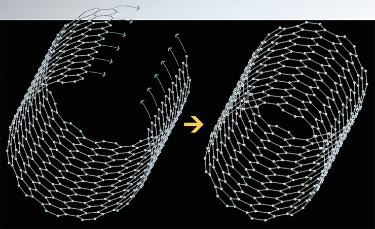
One of specific features typical of carbon nanotubes is their ability to emit electrons at relatively low intensities of the applied electric field (field emission). This phenomenon is promoted by the large ratio of the nanotube length to its diameter, which can reach 104. As the electric field intensifies near the nanotube end, the emission of electrons into vacuum can take place at the intensity of the applied field as low as 1 W/µm or less (Bonard et al., 2001). On the other hand, emission from traditional conducting materials requires the field intensity that is by 2—3 orders of magnitude higher.
Thus, it is possible to pass electric current through carbon nanotubes without mechanical attachment of a second contact. This can substantially enhance the efficiency of their use as a field cathode of illuminated panels (Yeletskii, 2002). In this case the operating voltages of cathodes made of such nanotubes can be dozens of times lower than in conventional molybdenum or silicon autoemission cathodes.
The curvature of the nanotube surface causes higher reactivity compared to a flat graphite sheet. This results in the chemical modification of the nanotubes for the purpose of making new nanometerials. For example, nanotubes can be used as a support for semiconductor nanoparticles (Eder, 2010). In the last two decades such nanoparticles have been called quantum dots. This name emphasizes the dependence of their optical and electrical properties on their size. As the characteristics of quantum dots can be tuned by varying their size, they can be used for constructing various optoelectronic devices – solar cells, light-emitting appliances, optical detectors, etc. (Nann & Skinner, 2011).
Usually quantum dots are grown by solution chemistry methods. Then they are distributed in a polymer film which is placed on the cathode. The main problems when using such polymers are low dispersion of the quantum dots and electrical interaction between them, as well as electrical contact between the film and the cathode. These problems can be largely solved if the conducting support with an array of carbon nanotubes with quantum dots formed at their ends is used as a cathode. In this case, the nanotube, which is a good conductor, will supply electrons to the semiconductor nanoparticle.
Today, cadmium chalcogenides (CdTe, CdSe, CdS) are most actively studied as potential quantum dots. Their nanocrystals emit photons under illumination or when subjected to an electric field. For instance, the IIC has developed a technique for forming cadmium sulfide nanoparticles on the surface of carbon nanotubes.
Similar studies began abroad several years ago. For example, hybrid materials consisting of nanotubes and semiconductor nanoparticles for application in the elements of solar cells were developed in the USA and China (Li et al., 2010). The novelty of the Russian design is that the obtained hybrid material has electroluminescent properties. So, it can be used, for instance, in illuminating devices.
Useful defects
Hybrid materials “CdS quantum dots – carbon nanotubes” can be synthesized by two traditional methods. For example, preformed semiconductor nanoparticles can be attached to the nanotubes using functional groups. In the other method a “nucleus” which will grow into a nanoparticle is created on the surface of a nanotube. Both methods include chemical modification of the carbon surface.
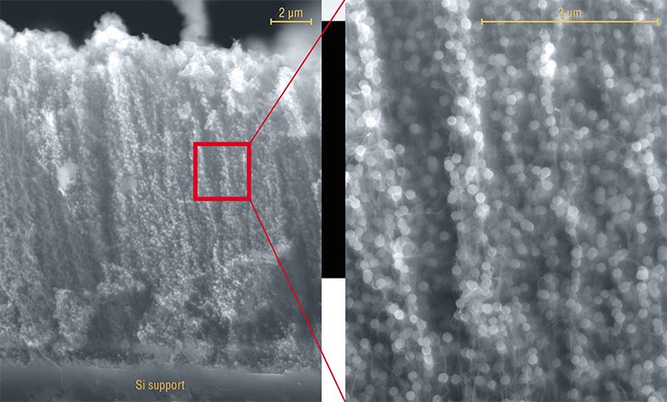
However, such modification is not required if in order to construct hybrid materials you use an array of nanotubes grown on silicon supports according to the method developed at the IIC. During catalytic decomposition of hydrocarbon vapors at temperatures of about 900 °C the surface of the nanotubes immediately acquires the necessary properties: these appear topological defects (carbon rings different from six-member ones) and vacancies (lack of one or several atoms in the crystal lattice).
Furthermore, often the morphology of nanotubes prepared by this method is different from a perfect cylinder. The graphite layers can be oriented at an angle to the nanotube axis, thus forming a structure consisting of nested cones. Carbon atoms at the edges of such a structure have a much higher reactivity compared to the atoms on an ideal graphite surface.
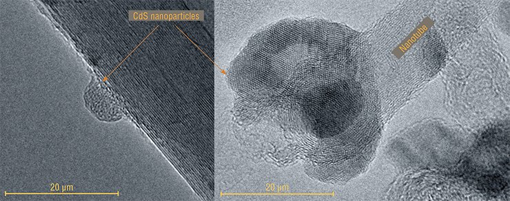
As a rule, toxic hydrogen sulfide or sodium sulfide is used for the industrial synthesis of cadmium sulfide. However, these reagents can be substituted for available low-toxic compounds which can supply a sulfur atom. For instance, about half a century ago a method for synthesizing CdS films from thiourea and cadmium chloride was developed at the IIC. A modified version of this method was used for developing nanohybrid photoluminescent materials (Kudashov et al., 2010).
 The examination of the obtained samples showed that roundish CdS nanoparticles were formed in the reaction solution at the ends and on the side surface of carbon nanotubes. The integrity of the array and the orientation of the nanotubes were preserved. The experiments demonstrated that the size of the nanoparticles could be varied by changing the temperature of the reaction mixture and the time of presence of the nanotubes in the solution.
At low synthesis temperatures rather uniform quantum dots were formed on the surface of the cathode. Nanoparticles grown in 5 minutes from a solution heated to 60 °C were spherical, had a narrow size distribution (150—200 nm) and were threaded on the nanotubes like beads. The latter fact indicates that the nucleus formation and growth of CdS nanoparticles take place directly on the surface of the carbon nanotube. Decreasing the reaction temperature to 30 °C and shortening the precipitation time to 1 minute led to the decrease of an average nanoparticle size to 20—30 nm.
Moreover, the surface of “conical” nanotubes appeared to be so active that precipitation of CdS nanoparticles occurred even at room temperature. It is worth mentioning, though, that under such conditions nanoparticles grow rather rarely, and apparently, only on the most defective sites of the surface such as the ends of nanotubes. However, it is these terminal nanoparticles that provide for the most efficient luminescence under exposure to an electrical field.
Shining like stars
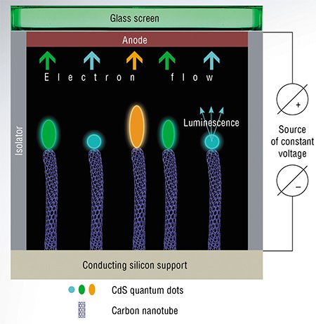
Using controlled cadmium sulfide precipitation, the Novosibirsk chemists managed to prepare a cathode from an array of carbon nanotubes, each containing a CdS nanoparticle at the end. When voltage is supplied to the conducting support, the electrical current flows through the nanotubes. As a result, high electric field density is created in the quantum dots at the ends of the nanotubes, which causes excitation of electrons in them. The lifetime of an excited system is about 10-10 s. Thereafter, the electron returns to the ground state. This transition is accompanied by the emission of a photon – electroluminescence takes place.
Images of a shining cathode are similar to those of stars in the sky, with the color of these “stars” being mostly green with rare orange spots. The predominance of green dots indicates that the crystal structure of CdS nanoparticles formed at the ends of the nanotubes is nearly perfect. Orange or red luminescence is usually attributed to the surface state with disrupted atom ordering (Tanno, 1998).
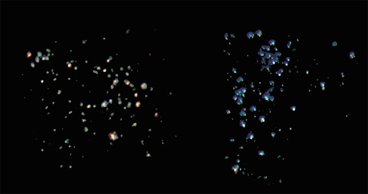
The colors green and red are conventional for cadmium sulfide luminescence. However, it is very difficult to obtain the blue color. So far there has been only one report on obtaining blue emission of CdS nanocrystals due to the combination of several electron transitions (Zhang, 2007). In this case, in order to mix the initial colors in required proportion the crystals were subjected to additional treatment for many hours.
Blue luminescence of CdS can also be obtained if regions with “ideal” atom ordering in the crystal lattice coexist with regions with a disordered location of atoms. Such “disorder” can be achieved by introducing a small amount of another metal into the crystal lattice.
Copper was chosen as such a “guest” because addition of Cu2+ salts to the reaction mixture that was used to grow the films was known to result in structural deformation of the CdS crystal lattice (Petre, 1999). Indeed, the experiments carried out at the IIC showed that quantum dots obtained by adding a small amount (10-4 mol/l) of copper chloride to the reaction solution luminesced mostly in blue.
Since the color of a luminescent quantum dot can be altered by varying the reaction conditions, luminescent elements of a wide color palette can be obtained. Such elements will be in great demand for developing light sources with a large surface area and low electric energy consumption. High current density will also allow one to obtain small-sized light sources of very high brightness.
If carbon nanotubes are grown on a special circuit rather than on a conducting support, it is possible to organize fast supply of electric energy to each individual semiconductor nanoparticle through the nanotube connected with it. The resolution of a display based on such “nanocircuit” will be higher by an order of magnitude than that of the existing devices.
References
Eleckij A.V. Uglerodnye nanotrubki i ih jemissionnye svojstva // Uspehi fizicheskih nauk. 2002. T. 172. C. 401—438.
Kudashov A.G. i dr. Sintez gibridnogo materiala iz nanochastic CdS i uglerodnyh nanotrubok // Izv. Akad. nauk. Serija himicheskaja. 2010. T. 9. S. 1674—1677.
Bonard J.-M. et al. Field emission from carbon nanotubes: the first five years // Solid-State Electronics. 2001. V. 45. P. 893—914.
Eder D. Carbon nanotube – inorganic hybrids // Chem. Rev., 2010. V. 110. P. 1348—1385.
Fregnaux M. et al. Physical and chemical analyses on single-source precursor-grown CdS semiconductor nanomaterials // J. Phys. Chem. C. 2010. V. 114. P. 17318—17323.
Li X. et al. Solar Cells and Light Sensors Based on Nanoparticle-Grafted Carbon Nanotube Films //ACS Nano. 2010. V. 4. No. 4. P. 2142—2148.
Iijima S. Helical microtubules of graphitic carbon // Nature. 1991. V. 354. P. 56—58.
This study was supported by the Russian Foundation for Basic Research (Grant 10-03-00696)


